CS201 Lab: Design Sequential Adders & Subtractors
Objectives
- Review the definition of half-adder and full adder
- Examine an binary adder-subtractor
- Investigate a 4-bit shift register and use it to store the results
- Build sequential adder, subtractor, and adder-subtractor circuits to verify the suquential design procedures
Half-Adder
    A Half-adder is a combinational circuit that performs the addition of 2 bits.

	Inputs: 	2 input bits to be added  (X, Y)

	Outputs: 	sum bit (S)
			carry bit (C)

    For example:

	1 + 1 = 1 0 		C = 1;  S = 0

	1 + 0 = 0 1		C = 0;  S = 1
Full-Adder
    A Full-adder is a combinational circuit that forms the arithmetic sum of 3 input bits.

	Inputs: 	2 input bits to be added (X, Y)
			1 carry bit from previous lower significant position (Ci)

	Outputs: 	sum bit (S)
			carry bit (Ci+1)

    For example:

	1 + 1 + 1 = 1 1 	Ci+1 = 1;  S = 1
	1 + 0 + 1 = 1 0		Ci+1 = 1;  S = 0

    Note: it takes 2 half-adders to make a full adder.


	Truth Table

	X   Y     Ci		Ci+1	    S
	------------------------------------------
	0   0	  0		0	    0
	0   0	  1		0	    1
	0   1	  0		0	    1
	0   1	  1		1	    0
	1   0 	  0		0	    1
	1   0	  1		1	    0
	1   1     0		1	    0
	1   1     1		1	    1
	-------------------------------------------

	Expressions

	S = X XOR Y XOR Ci
	Ci+1 = XY + Ci(X XOR Y)
Sequential Full-Adder
	State Table

	Inputs	PresentState	NextState   Output
	X   Y     Ci		Ci+1	    S
	------------------------------------------
	0   0	  0		0	    0
	0   0	  1		0	    1
	0   1	  0		0	    1
	0   1	  1		1	    0
	1   0 	  0		0	    1
	1   0	  1		1	    0
	1   1     0		1	    0
	1   1     1		1	    1
	-------------------------------------------

	The sequetial design
Full-Subtractor
   A Full-Subtractor is a combinational circuit that forms the arithmetic difference of 3 input bits.

   Inputs:  2 input bits to do subtraction (X, Y)
            1 borrow bit from previous lower significant position (Bi)

   Outputs:    Difference bit (D)
               Borrow bit (Bi+1)

   For example:

   1 - 1 - 1 = 1 1      Bi+1 = 1;  D = 1
   1 - 0 - 1 = 0 0      Bi+1 = 0;  D = 0

   Note: it takes 2 half-subtractors to make a full subtractor.


   Truth Table

   X   Y   Bi     Bi+1   D
   ------------------------------------------
   0   0   0      0      0
   0   0   1      1      1
   0   1   0      1      1
   0   1   1      1      0
   1   0   0      0      1
   1   0   1      0      0
   1   1   0      0      0
   1   1   1      1      1
   -------------------------------------------

   Expressions

   D = X XOR Y XOR Bi
   Bi+1 = X'Y + Bi(X XOR Y)'
Design and test a full subtractor (schematic diagram and truth table shown above).
A Sequential Full-Subtractor can be considered and designed the same way as a sequential Full-Adder for your lab assignment.
Binary Adder-Subtractor
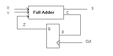
A binary adder is the circuit that generates the arithmetic sum of two binary numbers of any length. The subtraction of binary numbers can be done most conveniently by means of complements of numbers. Subtraction A - B can be done by taking the 2's complement of B and adding it to A. The 2's complement can be obtained by taking the 1's complement and adding 1 to the least significant pair of bits. The 1's complement can be implemented with inverters and a 1 can be added to the sum through the input carry. The addition and subtraction operations can be combined into one common circuit by including an exclusive-OR (XOR) gate with a full-adder. A bit sequential adder-subtractor is shown in the following figure:
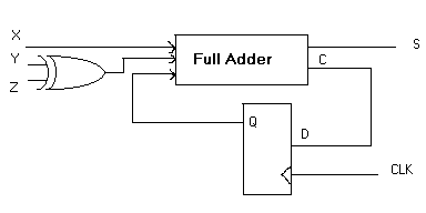
Input X is used to represent the bit of the binary number A. Input Y is used to represent the bit of the binary number B. The control signal Z controls the type of operation. When Z = 0 the circuit is an adder, meanwhile, the D flip-flop should be initialized to 0. When Z = 1 the circuit becomes a subtractor. The D flip-flop should be initialized to 1. The XOR gate receives input of signal bit Z and the input of the operand bit Y. When Z = 0, we have Y XOR Z = Y. ------------------------------------------------- The full adder receives the value of Y, the input carry is 0 because D flip-flop was initialized to 0, and the circuit performs A plus B. When Z = 1, we have Y XOR Z = Y' and the initial carry to 1. -------------------------------------------------------------------------------- The Y input is complemented and a 1 is added through the initial input carry. The circuit performs the operation: A plus the 2's complement of B. For unsigned numbers A and B, this gives the A - B if A >= B or 2's complement of (B - A) if A < B. For signed numbers, the result is A - B provided there is no overflow.
Introducing a 4-bit Shift Register:
Build the following circuit and get yourself familiar with the loading and shifting mode.
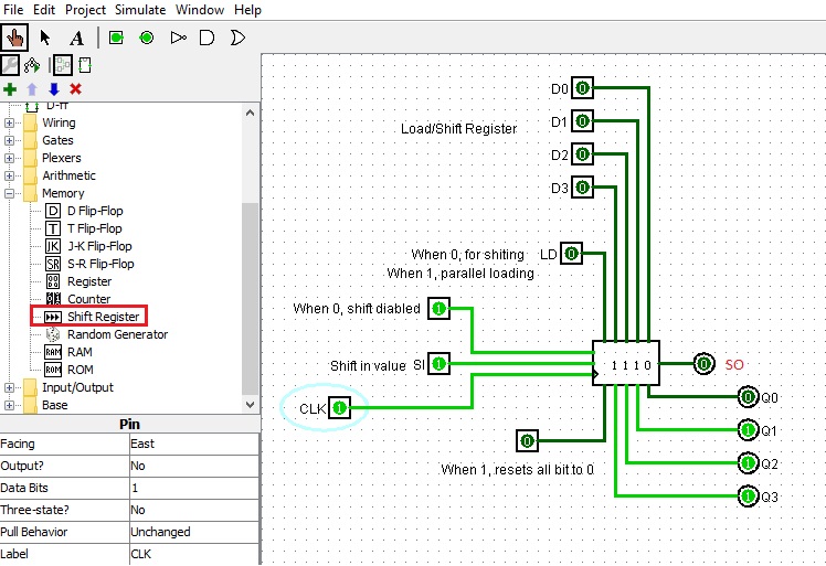
        It demonstrates the following:

                1.      How to use a 4 bit shift register.

                2.      How to use the Load and Shift modes.

                3.      How to show the values on each output bit to make
                        it easier to see what's happening in shift mode.

                4.      Shifting direction is SI->Q3->Q2->Q1->Q0 = SO.

        With LD set to 0:

                The register is in shift Right mode;
                The SI (shift in bit) line is used to set the value to be
                shifted into the register. Clocking is positive edge triggered.

        With LD set to 1:

                The register is in parallel load mode.
                Inputs D0 to D3 become outputs Q0 to Q3 on the next
                rising clock pulse.

        It can be used to store and diplay the output of your
	sequential adder, subtractor, and adder-subtractor circuits
	in the lab assignment.
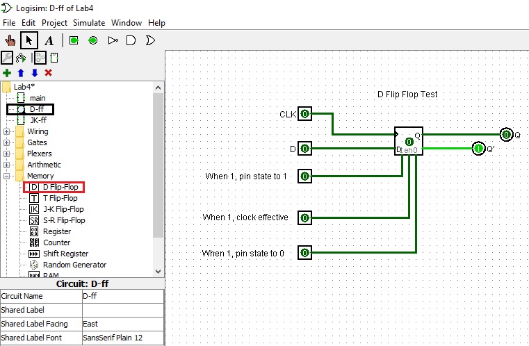
D flip flop review
The D flip-flop(shown below) lets the input at D propogate through to Q on the positive going edge of the clock. The present state-next state chart illustrates the behavior of the D flip-flop. Basically Q(t+1) = D, which is the characteristic equation.
	Characteristic Table		Excitation Table
	====================            ===================
	D  Q(t+1)  Operation            Q(t)  Q(t+1)   D
	====================		===================
	0    0     Reset                 0      0      0
	--------------------            -------------------
	1    1     Set                   0      1      1
	====================            -------------------
					 1      0      0
					-------------------
					 1      1      1
					===================