Build an 8-bit CPU
Objectives
- Learn the basic CPU structure and Organization
- Learn Memory, Registers, Tri-state Buffers and Decoders
- Build an 8-bit CPU with a memory
Through the building process, you will learn the CPU organization and learn how to use the memory.
Describing the CPU structure
In the above design/diagram, the following components have been added:
 <1.>PC - Program counter, use an 8-bit register for it
 <2.>PC+1 can be implemented by using an 8-bit ADDER to add a constant 00000001 to the PC.
 <3.>MAR - memory address register
 <4.>MEM - 8-bit memory


By now you have enough knowledge to build an 8-bit CPU without a memory.

We are going to introduce the memory below so that you will have enough knowledge to implement the above design.
Introducing 8-bit memory in Logisim
	When you build a CPU, you need a memory to hold the instructions,
	operands, etc. as shown in the CPU structure diagram.

	Here is a link to the RAM in the Logisim Memory Library for your reference.
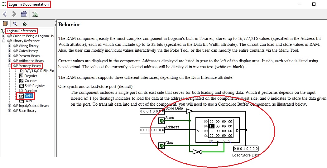
	Please read the document carefully and test the above given circuit for the RAM.

	This document can also be found in the Memory library
	in the Library reference in the Help menu in the Logisim.
Here is a demonstration of how to use an 8-bit memory in Logisim and it is helpful for you to build your 8-bit CPU with a memory.
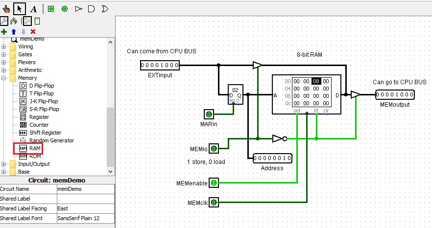
	Please build the circuit and try to operate on it with the following steps:


	Select 0x02(i.e. b00000010) from ETXin, Open EXTout,

	double click on MARin; close EXTout

	Select 0x08(i.e. b00001000) from EXTin, Open EXTout,

	Set MEMio to 1 to store value to the memory,

	Set MEMenable to 1 to be able to access the memory,

	double click on MEMclk; close EXTout

	Set MEMio to 0 to read the value.

	You just stored the number 0x08 in the memory location 0x02.
	And at the end,  you read the value in memory location 0x02.
Review 4-bit Parallel Adder
Look at the following circuit. It helps you to make an 8-bit PC+1.
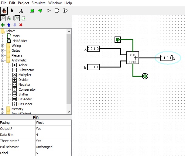
It demonstrates the following: 1. How to use the 4-bit inputs and outputs 2. How to use the 4 bit adder to obtain the sum The initial carry in Cin is 1-bit. The final carry out Cout is 1-bit.
Lab Assignment
Materials from last lab for your reference
We are going to keep the following lab materials for your reference.The following control signals will be required for our one bit CPU in this lab:In addition, an external input has been added to allow us to input values to the CPU bus for testing purposes. With the CPU built we will execute micro-operations to make the circuit execute instructions. Each register stores one bit of data and requires two control signals. Register-in loads the register with the contents of the bus. Register-out enables the tri-state buffer in the register which lets the register's output onto the bus. The ALU performs two operations, XOR and AND. The operation to be performed is to be determined by the code in the IR. A 0 in the IR indicates a XOR operation and a 1 indicates an AND operation.
        ACCout, ACCin, TEMPout, TEMPin, ALUout,

        IRin, Bout, Bin, Cout, Cin, EXTout.
A control unit would normally generate these control signals but
in our case input pins will be used for these control signals.
Registers
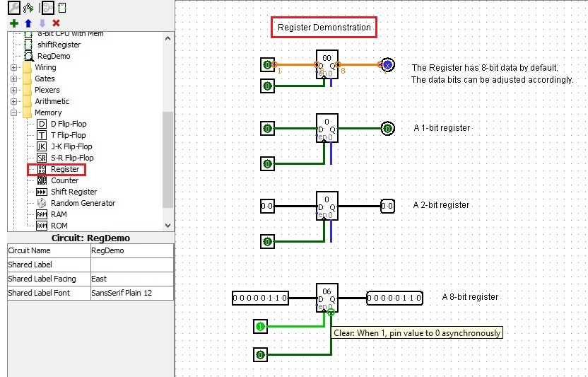
When you build a CPU, you need registers to hold the instruction, operands, etc. as shown in the CPU structure diagram.Here is a demonstration of how to use 1-bit, 2-bit, 8-bit registers.
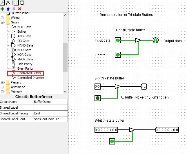
TRI-STATE BUFFER
In order to be able to build a CPU, we will have to look at how severalregisters/devices are connected to a common bus without causing short circuits and blown chips.
Imagine if one device is outputting a one and the other a 0 then what will be the output on bus? To avoid this problem we use a device called a tri-state buffer, which besides the states 0 and 1 has a floating third state.
These can be used to connect several devices to a bus and open one at a time. The tri-state buffers (or controlled buffers) are held in the floating state
except when that device wants to take control of the bus.
If more than one device tries to take control of the bus there will still be a conflict problem.
Here is a demonstration of using 1-bit, 2-bit, and 8-bit tri-state buffer:
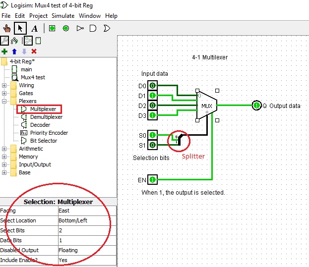
Multiplexers (MUX-4)
A multiplexer is a combinational logic circuit designed to select one of several input lines to a single common output line accordig to the selection control signals. For example, 2-1 Multiplexer has one control signal, 4-1 Mutiplexer has two control signals, 8-1 Multipleaxer has three control signals and so on.Here is a demonstration of 4-1 Multilexer with four input lines D0, D1, D2, D3 for your reference. This device can be used as the control unit of your 2-bit or 8-bit CPU circuit.
        Truth Table of a 4-1 Multiplexer (MUX 4)
        ========================================
        Input   Selection Output
        ----------------------------------------
                S1  S0      Q
        D0      0   0       D0
        D1      0   1       D1
        D2      1   0       D2
        D3      1   1       D3
        -----------------------------------------
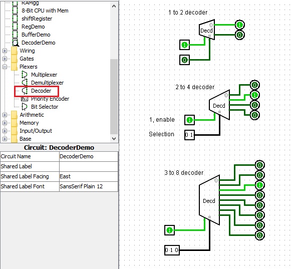
Decoders
A docoder could serve as the control unit for your CPUs. It is worthwhile to investigate the the decoders.
Build a 1-bit CPU
Many devices may be connected to a common bus by using tri-state buffers.
You may build a 1-bit CPU as described above to get a feel about it.
Here is a picture of the 1-bit CPU circuit for your reference.
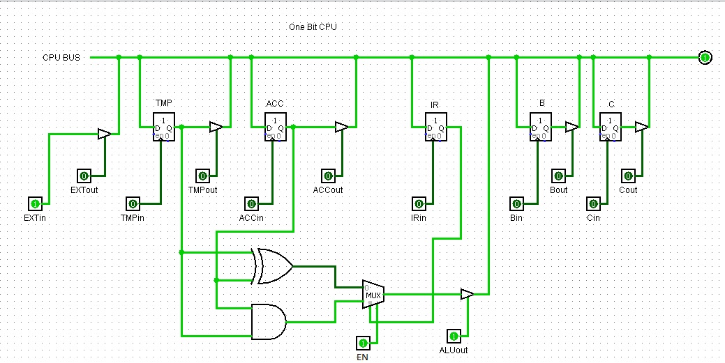
- In the above 1-bit CPU , What are control signals EXTout and Cin for?
- Design the bove 1-bit CPU descriped in the section one of the lab notes and implement the circuit.
Here are Some Relevant Details:
The ALU performs two operations, XOR and AND. The operation to be performed is to be determined by the code in the IR. The value 0 in the IR indicates an XOR operation and the value 1 indicates an AND operation.
The following control signals will be required for our 1-bit CPU in this lab:
ACCout, ACCin, TMPout, TMPin, ALUout, IRin, Bout, Bin, Cout, Cin, EXTout, EXTin. - To implement the operation AND, let's assume that
it uses the operands in registers B and C, and then stores the result in C.
The following instructions would have to be executed.
(assume the external input pin is set to the value '1' - the pre-condition for the AND operation):
And of course, register B and C should be pre-loaded with desired values.At the beginning, set all the "out" pins to '0' so that the bus will be available for use without conflicts. After each use, set all the "out" pins to '0' again to get ready for the next use. 1. EXTin, EXTout, IRin. // Load '1' in register IR for AND operation. 2. EXTin, EXTout, Bin. // Load '0' in register B. 3. EXTin, EXTout, Cin. // Load '1' in register C. 4. Bout, ACCin. 5. Cout, TMPin. 6. ALUout, Cin. 7. Cout.Practice these microinstructions with your newly built 1-bit CPU. -
Do the following experienment:
        Write out the steps necessary to implement the operation XOR
        that uses the operands in the accumulator and register C, and then
        stores the result in register B.